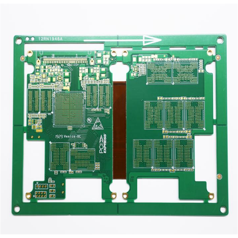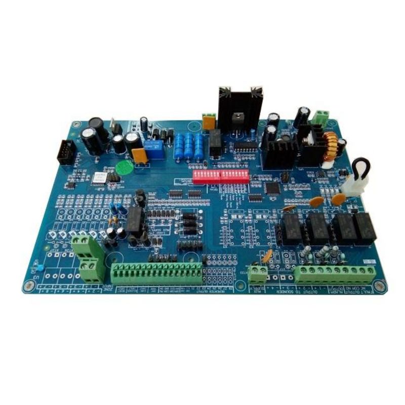
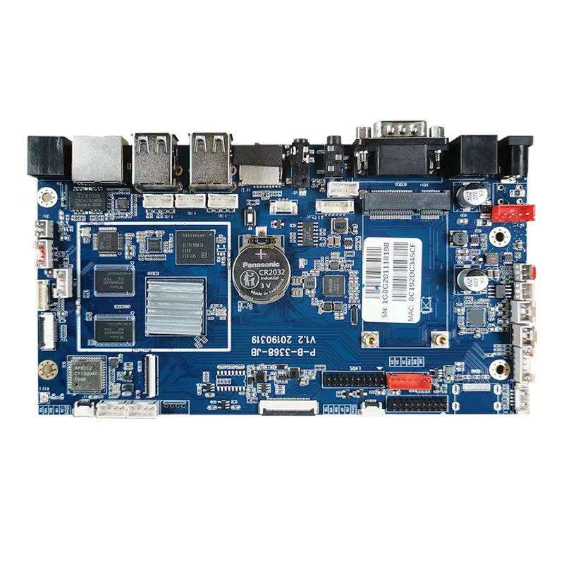


Product Specification:
| Layer | 6 layers |
| Material | FR-4 |
| Copper Thickness (in OZ) | 1OZ |
| Finish Board Thickness | 1.6 mm±0.1mm |
| Solder Mask | Green |
| Silkscreen | White |
| Surface Finish | HASL |
| Minimum line width and line spacing | 4/5 mil |
PCB assembly OEM service
- Electronic components material purchasing.
- Bare PCB fabrication.
- PCB Assembly Service. (SMT, BGA, DIP).
- FULL Test: AOI, In-Circuit Test (ICT), Functioal Test (FCT).
- Cable, Wire-harness assembly,sheet metal,Electrical cabinet Assembly service.
- Conformal coating service.
- Prototyping and mass production...

| FOB Port | Shenzhen |
| Weight per Unit | 10.0 Grams |
| HTS Code | 8534.00.90 00 |
| Export Carton Dimensions L/W/H | 44.0 x 30.0 x 34.0 Centimeters |
| Logistics attributes | Common |
| Lead Time | 7–15 days |
| Dimensions per Unit | 10.0 x 5.0 x 0.16 Centimeters |
| Units per Export Carton | 5000.0 |
| Export Carton Weight | 5.0 Kilograms |
Main Export Markets

- - Asia
- - Australasia
- - Central/South America
- - Eastern Europe
- - Mid East/Africa
- - North America
- - Western Europe
FAQs
| Value | Specification |
| Material | FR-4,FR1, CEM-1, CEM-3,Aluminum, Ceramic, Metal-backed Laminate, etc.Also make Crockery, Taconic, Rogers PCBs etc. |
| Remarks | High Tg CCL is Available(Tg>=170℃) |
| Finish Board Thickness | 0.2 mm-6.00mm(8mil-126mil) |
| Surface Finish | Gold finger(>=0.13um), Immersion Gold(0.025-0075um), Plating Gold(0.025-3.0um), HASL(5-20um), OSP(0.2-0.5um) |
| Shape | Routing、Punch、V-cut、Chamfer |
| Surface Treatment | Solder Mask(black, green, white, red, blue, thickness>=12um, Block, BGA) |
| Silkscreen(black, yellow, white) | |
| Peel able-mask(red, blue, thickness>=300um) | |
| Minimum Core | 0.075mm(3mil) |
| Copper Thickness | 1/2 oz min; 12oz max |
| Min Trace Width & Line Spacing | 0.075mm/0.1mm(3mil/4mil) |
| Min Hole Diameter for CNC Drilling | 0.1mm(4mil) |
| Min Hole Diameter for Punching | 0.6mm(35mil) |
| Biggest panel size | 610mm * 508mm |
| Hole Position | +/-0.075mm(3mil) CNC Drilling |
| Conductor Width(W) | +/-0.05mm(2mil) or +/-20% of original |
| Hole Diameter(H) | PTHL:+/-0.075mm(3mil) |
| Non PTHL:+/-0.05mm(2mil) | |
| Outline Tolerance | +/-0.1mm(5mil) CNC Routing |
| Warp & Twist | 0.70% |
| Insulation Resistance | 10Kohm-20Mohm |
| Conductivity | <50ohm |
| Test Voltage | 10-300V |
| Panel Size | 110 x 100mm(min) |
| 660 x 600mm(max) | |
| Layer-layer misregistration | 4 layers:0.15mm(6mil)max |
| 6 layers:0.25mm(10mil)max | |
| Min spacing between hole edge to circuitry pattern of an inner layer | 0.25mm(10mil) |
| Min spacing between board outline to circuitry pattern of an inner layer | 0.25mm(10mil) |
| Board thickness tolerance | 4 layers:+/-0.13mm(5mil) |