Overview
- Electronic components material purchasing.
- Bare PCB fabrication.
- PCB Assembly Service. (SMT, BGA, DIP).
- FULL Test: AOI, In-Circuit Test (ICT), Functioal Test (FCT).
- Cable, Wire-harness assembly,sheet metal,Electrical cabinet Assembly service.
- Conformal coating service.
- Prototyping and mass production...
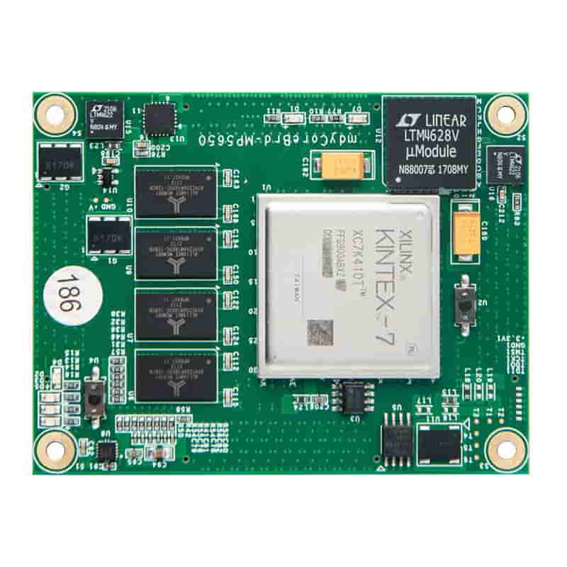
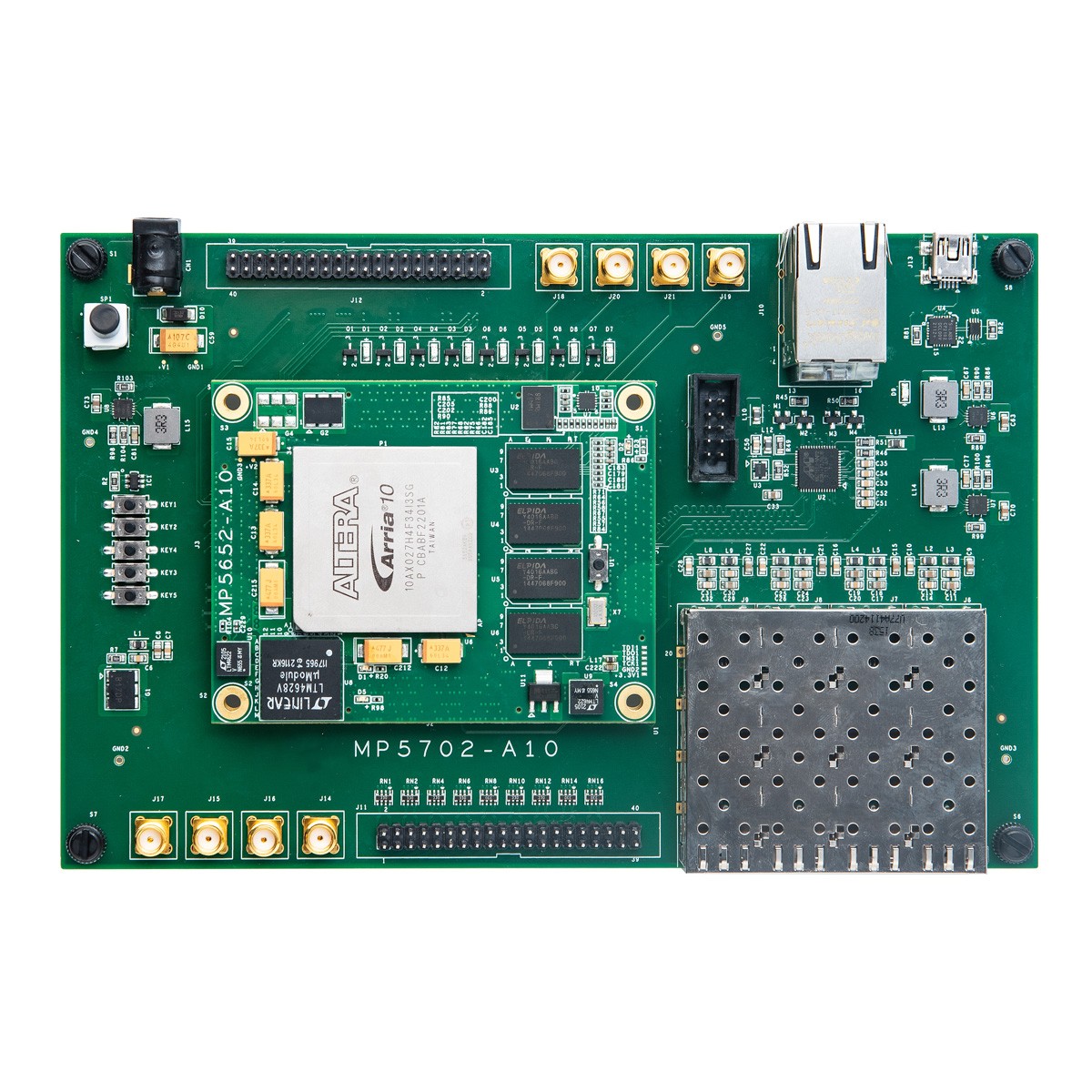
 DDR3 SDRAMQ: 16GB DDR3, 4GB per piece, 16bit Data Bit Data Bid SPI Flash: One piece of 128MBITQSPIFLASH, which can be used for FPGA configuration files and user data storage FPGA Bank interface levels: adjustable 1.8V, 2.5V, 3.3V electrical If you need to replace the level, you only need to replace the corresponding position of the magnetic bead to achieve adjustment. Core board power supply: 5V-12V range of power supply EEPROM; M24C02-WMN6TP is based on I2C bus device. Following the starting method of the core board of the second-line protocol: supports two start-up modes, which are JTAG, QSPI Flash connectors. Extended port, 120pin, Panasonic AXK5A2137yg MP5700 bottom plate SFP interface: 2 optical modules can achieve high -speed optical fiber communication, as high as 6GB/s bottom plate clock: 1 200MHz reference clock connected to the core board MRCC clock tube foot, 1 125MHz The GTX clock tube feet bottom plate of the clock connect to the core board is 40 -pin expansion port: reserve a 2.54mm standard spacing 40 -shot extension port, which is used to connect the customer's own design module. Essence Core board clock: there are multiple clock sources on the board. These include the 200MHz system clock, the 125MHz GTX clock, and the 66MHz EMCCLK clock. JTAG port: 10 stitches 2.54mm standard JTAG port, for downloading and debugging LEDs for FPGA programs: a total of 6 red LED lights in the core board, indicating the power supply of the board card, 4 signal indicator lights and FPGA IO tube feet directly connected directly Key: 4 keys. 4 keys. They are FPGA reset buttons, Program_b keys and two user keys
- Electronic components material purchasing.
- Bare PCB fabrication.
- PCB Assembly Service. (SMT, BGA, DIP).
- FULL Test: AOI, In-Circuit Test (ICT), Functioal Test (FCT).
- Cable, Wire-harness assembly,sheet metal,Electrical cabinet Assembly service.
- Conformal coating service.
- Prototyping and mass production...
FAQs

